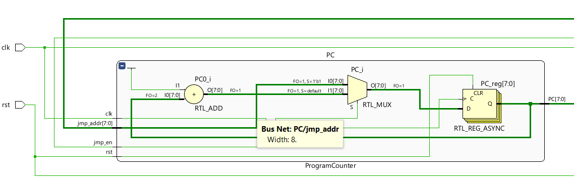
1) Program Counter (PC)
The Program Counter (PC) is responsible for storing the address of the current instruction being executed by the CPU. After every instruction, it increments automatically to point to the next instruction in memory.
- Holds the current instruction address
- Automatically increments every clock cycle
- Supports branching and jumping (future enhancement)
- Synchronous update using clock and reset
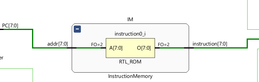
2) Instruction Memory
Instruction Memory stores the machine instructions executed by the CPU. The Program Counter supplies the address, and the memory outputs the corresponding instruction every cycle.
- Stores 8-bit instructions
- Addressed using the Program Counter
- Preloaded with instructions during simulation
- Combinational read operation
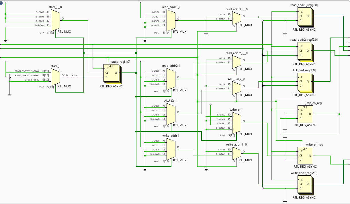
3) Control Unit (FSM)
The Control Unit decodes the instruction and generates control signals required by the ALU and Register File. It operates as a simple three-state FSM: FETCH → DECODE → EXECUTE.
- Decodes opcode from instruction
- Generates ALU selection signals
- Selects register addresses for read/write
- Asserts write enable during EXECUTE state
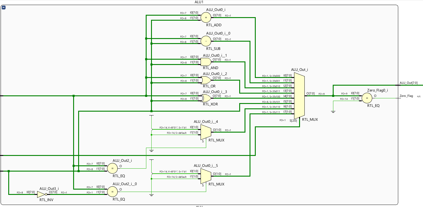
4) Arithmetic Logic Unit (ALU)
The ALU performs all arithmetic and logical operations of the CPU. It takes two 8-bit inputs and produces an 8-bit output based on the selected operation.
- Supports ADD, SUB, AND, OR, XOR
- Zero flag generation
- Operates based on ALU_Sel control lines
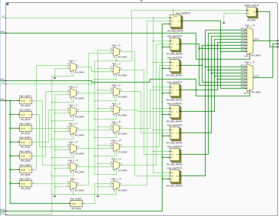
5) Register File
The Register File stores temporary values used by the CPU during instruction execution. It includes two read ports and one write port.
- Contains 8 registers (8-bit each)
- Two read ports for ALU input
- One write port controlled by Control Unit
- Registers reset on system reset
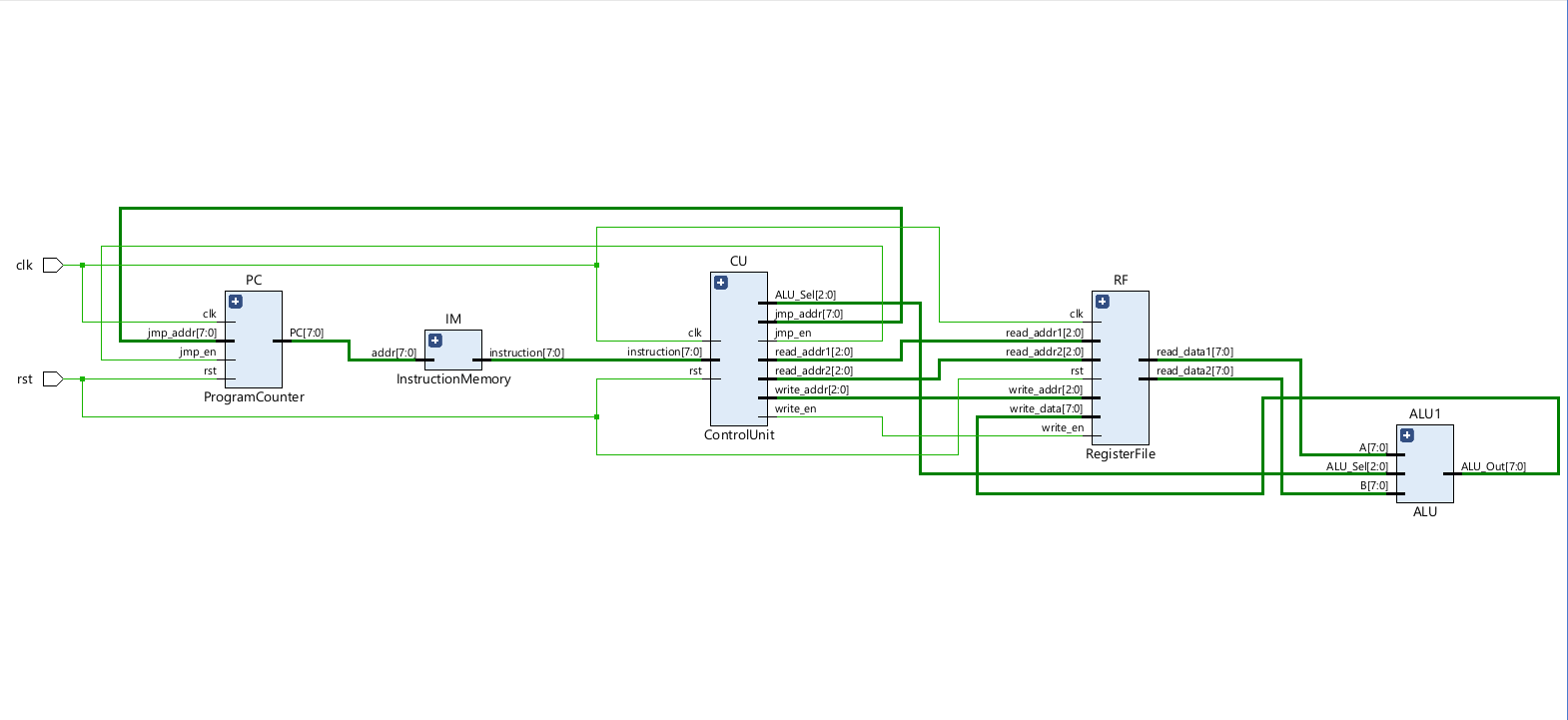
6) Full 8-bit RISC CPU
The complete CPU integrates the Program Counter, Instruction Memory, Control Unit, Register File, and ALU into a functioning RISC datapath.
- Implements Fetch → Decode → Execute cycle
- All modules connected through shared datapath
- Simulated in Xilinx Vivado using testbench
- Produces waveforms for each instruction
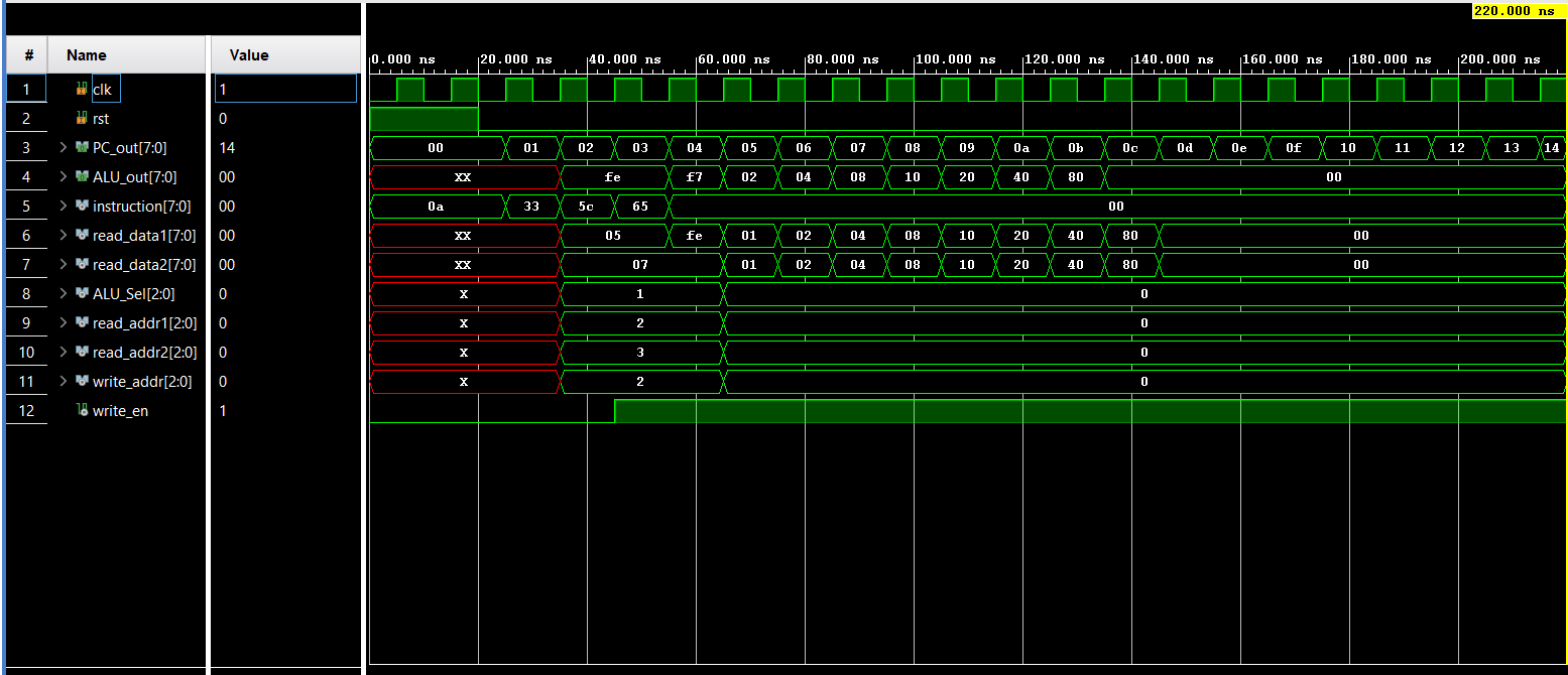
7) Testbench for 8-bit RISC CPU
The testbench is used to verify the functionality of the 8-bit RISC CPU. It generates the clock and reset signals, loads sample instructions, and observes the waveform outputs for correct ALU operations and control signal transitions. The testbench ensures the processor executes the Fetch → Decode → Execute cycle correctly.
- Generates 10ns clock signal
- Applies reset pulse
- Runs CPU for multiple cycles
- Monitors instruction flow and ALU output
Source Code including testbench
1. ALU (Arithmetic Logic Unit)
module ALU (
    input  [7:0] A, B,       // Operands
    input  [2:0] ALU_Sel,    // ALU operation select
    output reg [7:0] ALU_Out,
    output reg Zero_Flag
);
always @(*) begin
    case (ALU_Sel)
        3'b000: ALU_Out = A + B;          // ADD
        3'b001: ALU_Out = A - B;          // SUB
        3'b010: ALU_Out = A & B;          // AND
        3'b011: ALU_Out = A | B;          // OR
        3'b100: ALU_Out = A ^ B;          // XOR
        3'b101: ALU_Out = B;              // MOV
        3'b110: ALU_Out = (A == B) ? 8'd1 : 8'd0; // CMP
        3'b111: ALU_Out = (A == ~B) ? 8'd1 : 8'd0; // CMP NEGATIVE
        default: ALU_Out = 8'd0;
    endcase
    Zero_Flag = (ALU_Out == 8'd0);
end
endmodule
2. Register File
module RegisterFile (
    input clk, rst,
    input write_en,
    input [2:0] read_addr1, read_addr2, write_addr,
    input [7:0] write_data,
    output [7:0] read_data1, read_data2,
    output reg [7:0] regfile
);

reg [7:0] regs [7:0]; // 8 registers (R0-R7)
assign read_data1 = regs[read_addr1];
assign read_data2 = regs[read_addr2];

always @(posedge clk or posedge rst) begin
    if (rst)
        regs[0] <= 8'd0; // Reset R0
    else if (write_en)
        regs[write_addr] <= write_data;
end

integer i;
always @(posedge rst) begin
    for (i = 0; i < 8; i = i + 1)
        regfile[i] <= 8'd0;
end

endmodule
3. Program Counter
module ProgramCounter (
    input clk, rst,
    input jmp_en,
    input [7:0] jmp_addr,
    output reg [7:0] PC
);

always @(posedge clk or posedge rst) begin
    if (rst)
        PC <= 8'd0;
    else if (jmp_en)
        PC <= jmp_addr;
    else
        PC <= PC + 1;
end

endmodule
4. Instruction Memory
module InstructionMemory (
    input [7:0] addr,
    output reg [7:0] instruction
);

reg [7:0] memory [0:255];
initial begin
    memory[0] = 8'b000_001_010;  // ADD R1, R2
    memory[1] = 8'b001_010_011;  // SUB R2, R3
    memory[2] = 8'b010_011_100;  // AND R3, R4
    memory[3] = 8'b011_100_101;  // OR  R4, R5
    memory[4] = 8'b000_000_000;  // NOP
end

always @(*)
    instruction = memory[addr];

endmodule
5. Control Unit (FSM)
module ControlUnit (
    input clk, rst,
    input [7:0] instruction,
    output reg [2:0] ALU_Sel,
    output reg [2:0] read_addr1, read_addr2, write_addr,
    output reg write_en,
    output reg jmp_en,
    output reg [7:0] jmp_addr
);

reg [1:0] state;
parameter FETCH=2'd0, DECODE=2'd1, EXECUTE=2'd2;

always @(posedge clk or posedge rst) begin
    if (rst) begin
        state <= FETCH;
        write_en <= 0;
        jmp_en <= 0;
    end
    else begin
        case (state)
            FETCH: state <= DECODE;

            DECODE: begin
                ALU_Sel   <= instruction[7:5];
                write_addr<= instruction[4:3];
                read_addr1<= instruction[4:3];
                read_addr2<= instruction[2:0];
                state     <= EXECUTE;
            end

            EXECUTE: begin
                write_en <= 1;
                state    <= FETCH;
            end
        endcase
    end
end

endmodule
6. CPU Top Module
module CPU_Top (
    input clk, rst
);

wire [7:0] instruction, PC_out;
wire [7:0] read_data1, read_data2, ALU_out;
wire [2:0] ALU_Sel, read_addr1, read_addr2, write_addr;
wire write_en, jmp_en;
wire [7:0] jmp_addr;
wire Zero_Flag;

// Instantiate modules
ProgramCounter PC(clk, rst, jmp_en, jmp_addr, PC_out);
InstructionMemory IM(PC_out, instruction);
ControlUnit CU(clk, rst, instruction, ALU_Sel, read_addr1, read_addr2, write_addr, write_en, jmp_en, jmp_addr);
RegisterFile RF(clk, rst, write_en, read_addr1, read_addr2, write_addr, ALU_out, read_data1, read_data2);
ALU ALU1(read_data1, read_data2, ALU_Sel, ALU_out, Zero_Flag);

endmodule
7. Testbench
`timescale 1ns/1ps

module tb_RISC_CPU;

reg clk;
reg rst;

wire [7:0] alu_out;
wire [7:0] instr;
wire [2:0] alu_sel;
wire write_en;
wire [2:0] read_addr1, read_addr2, write_addr;
wire jmp_en;
wire [7:0] jmp_addr;

// Instantiate CPU
RISC_CPU uut (
    .clk(clk),
    .rst(rst),
    .alu_out(alu_out),
    .instruction(instr),
    .ALU_Sel(alu_sel),
    .write_en(write_en),
    .read_addr1(read_addr1),
    .read_addr2(read_addr2),
    .write_addr(write_addr),
    .jmp_en(jmp_en),
    .jmp_addr(jmp_addr)
);

// Clock
always #5 clk = ~clk;

initial begin
    clk = 0;
    rst = 1;
    #20 rst = 0;
    #200;
    $stop;
end

initial begin
    $monitor("Time=%0t | Instr=%b | ALU_Sel=%b | ALU_Out=%b | W_En=%b",
             $time, instr, alu_sel, alu_out, write_en);
end

endmodule